A Comprehensive Guide to ASIC Design Flow
Application-Specific Integrated Circuits (ASICs) are custom-designed chips tailored for specific applications, offering optimized performance, power, and area compared to general-purpose processors. The ASIC design flow is a complex and multi-stage process involving various steps, from initial specification to final fabrication and verification. This guide provides an in-depth look at the entire ASIC design flow, detailing each phase and the associated tasks and methodologies.
1.1. Definition:
- Purpose: Determine the functionality and performance requirements of the ASIC.
- Tasks:
- Functional Specification: Define what the ASIC is supposed to do, including features, performance metrics, and interfaces.
- Performance Requirements: Specify speed, power consumption, and area constraints.
- Interface Requirements: Define how the ASIC will interact with other components or systems.
- Verification Requirements: Establish how the design will be tested to ensure it meets specifications.
1.2. Documentation:
- Create a comprehensive specification document that serves as the blueprint for the design and verification processes.
2. Architectural Design
2.1. High-Level Design:
- Purpose: Develop the high-level architecture of the ASIC.
- Tasks:
- Architecture Definition: Create a block diagram representing the major functional blocks and their interactions.
- Design Partitioning: Divide the design into manageable blocks or modules, considering reuse and modularity.
- Performance Analysis: Estimate the performance of the design and refine architecture as needed.
2.2. System-Level Design:
- Purpose: Develop a more detailed design and plan for integrating the functional blocks.
- Tasks:
- Interface Design: Define communication protocols and interfaces between different blocks.
- Data Path and Control Path: Design the data path (e.g., arithmetic units) and control path (e.g., state machines).
- Power and Clock Planning: Define power distribution and clocking strategies.
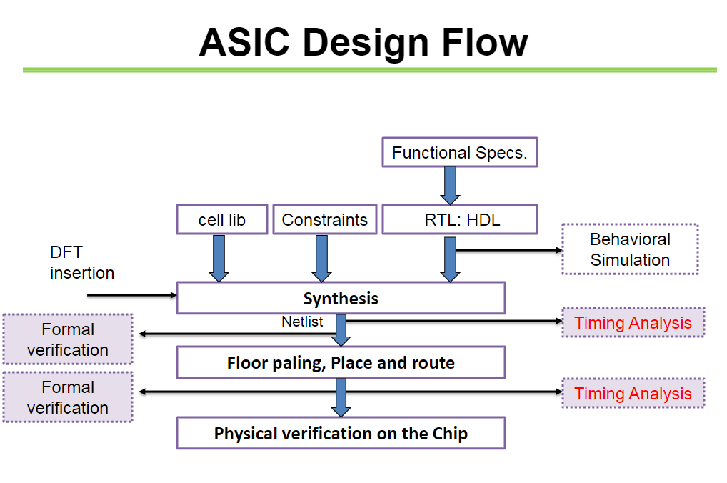
3. RTL Design
3.1. Register Transfer Level (RTL) Design:
- Purpose: Develop the RTL code that describes the behavior and structure of the ASIC.
- Tasks:
- HDL Coding: Write the design description using Hardware Description Languages (HDLs) like Verilog or VHDL.
- Functional Simulation: Test the RTL code with simulations to verify that it meets the functional specifications.
- Synthesis Constraints: Define constraints for synthesis to guide the transformation from RTL to gate-level representation.
3.2. RTL Verification:
- Purpose: Ensure that the RTL design functions correctly.
- Tasks:
- Testbenches: Develop testbenches to validate the RTL design.
- Formal Verification: Use formal methods to prove the correctness of the RTL design.
4. Synthesis
4.1. Logic Synthesis:
- Purpose: Convert RTL code into a gate-level netlist.
- Tasks:
- Synthesis Tool: Use synthesis tools (e.g., Synopsys Design Compiler) to transform RTL code into a gate-level representation.
- Constraint Setting: Apply constraints such as timing, area, and power to guide the synthesis process.
- Optimization: Optimize the design for performance, area, and power.
4.2. Post-Synthesis Verification:
- Purpose: Verify that the synthesized design meets the specifications.
- Tasks:
- Functional Verification: Ensure that the synthesized design still meets functional requirements.
- Timing Analysis: Perform static timing analysis to ensure that the design meets timing constraints.
5. Physical Design
5.1. Floorplanning:
- Purpose: Define the physical layout of the design blocks on the chip.
- Tasks:
- Placement: Place functional blocks on the chip according to design constraints and requirements.
- Power Planning: Define the power grid and ensure sufficient power distribution.
5.2. Routing:
- Purpose: Connect the placed blocks with interconnecting wires.
- Tasks:
- Global Routing: Plan the overall routing to connect blocks.
- Detailed Routing: Finalize the routing with specific metal layers and connections.
OUR PLACEMENT PARTNERS


Subscribe to our newsletter to recieved the latest udates and information about codehauz
All rights reserved (C) 2024 Innovative-hub for VLSI Technology